Time:2022-09-18 Views:
In order to curb China's technological development, the United States has increasingly used national power in recent years to maintain its technological hegemony through various "malicious restrictions". For example, it has repeatedly tightened the export of semiconductor equipment to China, frequently expanded the technology export control list, and prohibited ASML from selling DUV lithography machines with 14nm and below processes to my country, and even extended the magic to Chinese scientists.
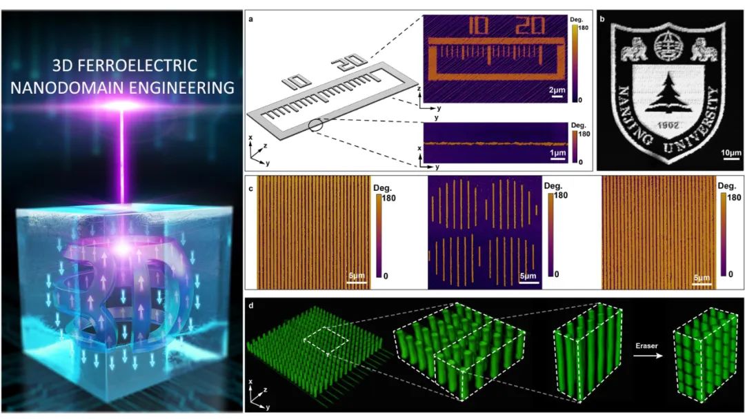
However, in the face of these "stuck neck" technical problems, China not only did not choose to give in, but instead embarked on its own unique development path. No, good news just came from the domestic independent chip industry: on the evening of September 14, the world's top academic journal "Nature" published a new study. Chinese scientists have obtained nano-scale light-engraving three-dimensional structures for the first time. In the next generation Major breakthroughs have been made in the field of optoelectronic chip manufacturing.
It is reported that the scientific research team led by Zhang Yong, Xiao Min and Zhu Shining of Nanjing University has invented a new technology of "non-reciprocal femtosecond laser polarized ferroelectric domain", which focuses the femtosecond pulsed laser on the material "lithium niobate". Inside the crystal, by controlling the direction of laser movement, an effective electric field is formed inside the crystal to realize direct writing and erasing of three-dimensional structures.
The difficulty of this technology is that it breaks through the light diffraction limit of traditional femtosecond lasers, and reduces the size of the three-dimensional structure of light-engraved lithium niobate from the traditional 1μm order (equivalent to one-fifth of the hair) for the first time. To the nanometer level, up to 30nm, which greatly improves the processing accuracy.
The study pointed out that this major invention may open up a new track for optoelectronic chip manufacturing in the future, and is expected to be used in the preparation of key optoelectronic device chips such as optoelectronic modulators, acoustic filters, and non-volatile ferroelectric memories. It has broad application prospects in the fields of computing and artificial intelligence.
We all know that chips, as the crystallization of the development of contemporary science and technology, play an irreplaceable and important role in military, civil and other fields. However, with the continuous development of integrated circuits, traditional electronic integrated circuits are gradually approaching their limits in terms of bandwidth and energy consumption, and the shipment of DUV/EUV lithography machines is limited. Therefore, as an important segment of the global semiconductor industry, optoelectronic chips are considered by the industry as the "most promising successor".

In simple terms, an optoelectronic chip is a highly integrated component. The integrated components include lasers, modulators, couplers, beam splitters, wavelength division multiplexers, detectors, etc., which are mainly used to complete photoelectric signal conversion. of.
In principle, electronic integrated chips use current signals as information carriers, while optoelectronic chips use higher-frequency light waves as information carriers. Compared with electronic integrated circuits or electrical interconnect technologies, photonic integrated circuits and optical interconnects exhibit lower transmission loss, wider transmission bandwidth, smaller time delay, and stronger anti-electromagnetic interference capabilities.
In addition, optical interconnection can improve the communication capacity within the transmission medium by using multiple multiplexing methods (such as wavelength division multiplexing WDM, mode division interoperability MDM, etc.). Therefore, on-chip optical interconnects based on integrated optical circuits are considered to be a promising technology, and optoelectronic chips can be used to overcome the bottleneck problem caused by electron transport.
It is reported that in order to break the limitations of Microchip, Huawei has already set its sights on optoelectronic chips. In the past two years, it not only spent 1 billion pounds to build an optoelectronics R&D center in Cambridge, England, but also recruited a large number of top foreign talents to develop optoelectronic chips for it. .
Earlier, Huawei founder Ren Zhengfei said that optoelectronic chips can completely bypass the US technology blockade. In other words, since the manufacturing process of optoelectronic chips is different from that of silicon chips, even if there is no EUV lithography machine, as long as we can master this technology, we can still mass-produce chips of 7nm and below!
Skype:szmyxdz@163.com
Tel: +86-13530718420
Email: szmyxdz@163.com
Company Homepage:en.icmyx.com
Working Hours:Monday To Saturday 00:00-24:00
 +86-13530718420
Skype:szmyxdz@163.com
E-Mail:szmyxdz@163.com
Company Address:A309-s31604, Rongchao economic and Trade Center, No. 4028, Jintian Road, Fuzhong community, Lianhua street, Futian District, Shenzhen

官方二维码
Links:
Copyright 2022 Shenzhen Meiyu core technology Co., Ltd Telephone:+86-13530718420 Guangdong ICP No. 2022094269-1

Service Hotline

Monday To Saturday 00:00-24:00

Skype

szmyxdz@163.com