Time:2022-10-25 Views:
As we all know, in the field of integrated circuits, its correct name is 7nm process technology, or 7nm process. It means that in an integrated circuit (chip), the size of a component can be as small as 7nm. In other words, the 16nm process means that the components can reach 16nm size. And the smaller the component size, the more advanced the technology and the more difficult it will be to manufacture.
Compared with some mainstream 10nm, 14nm and 16nm processes, if an integrated circuit (chip) of the same size uses a 7nm process, the number of electronic components on the chip will be more, so the performance will be stronger. At the same time, power consumption and heat generation will be reduced. Overall, 7nm represents stronger performance with lower power consumption and heat generation.

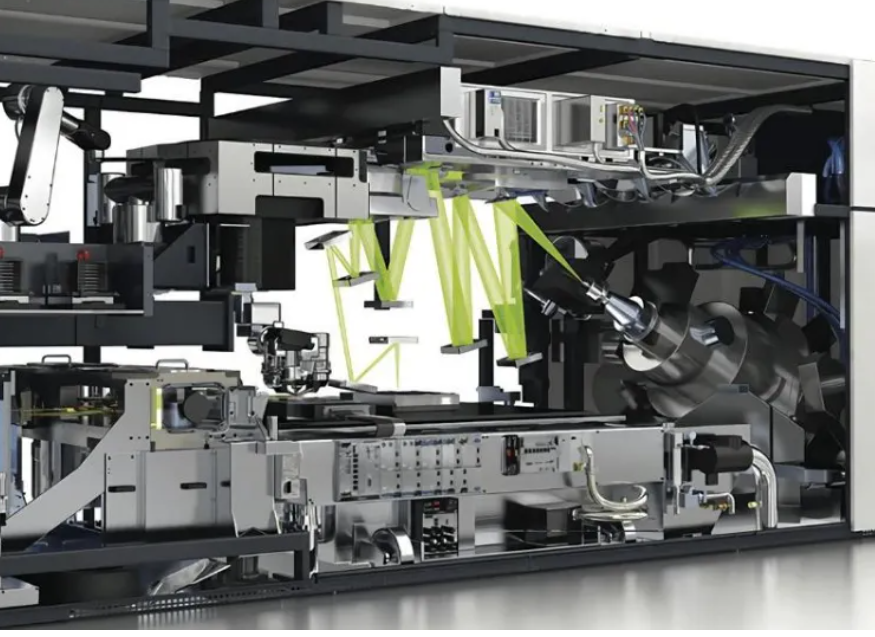
In the current semiconductor industry, lithography equipment that can support the 7nm process node is a highly complex device involving numerous key components such as high-performance light sources, precision optics, and precise metrology. It is understood that the equipment planned by the Russian institute is different from the lithography machines produced by companies such as ASML or Nikon. For example, the Russian Institute plans to use a light source greater than 600W (total power, not intermediate focus power) with an exposure wavelength of 11.3nm (13.5nm for EUV), which will require more complex optics than today. Since the device's light source power is relatively low, this will make the tool more compact and easier to manufacture. However, this also means that its scanners will have significantly lower yields than modern deep ultraviolet (DUV) tools. But in IAP's view, this may not be a problem.
Referring to the time point of "construction by 2028", IAP is very optimistic. Referring to the research and development process of the world's major head lithography machine manufacturers: ASML launched its first immersion lithography system at the end of 2003 - Twinscan XT: 1250i, and plans to deliver one in the third quarter of 2004 to produce 65nm logic chips and 70nm half-pitch DRAM. It took the company about five years to release the 32nm-capable Twinscan NXT: 1950i in late 2008, with customer deliveries starting in 2009.
Then it took ASML about nine more years to launch the Twinscan NXT:2000i DUV lithography machine with 7nm and 5nm capabilities in 2018. Taken together, it took ASML nearly 14 years to develop from 65nm to 7nm. It can be seen how difficult it is to improve the advanced technology.
Shenzhen Meiyuxin Technology Co., Ltd. sincerely invites suppliers to settle in Meiyuxin Mall! ! !
In this regard, Nikolai Chihalo, deputy director of the Institute of Microstructural Physics of the Russian Academy of Sciences responsible for scientific and technological development, said: "ASML is a global leader in lithography and has been developing its EUV lithography system for nearly 20 years. The technology proved to be extremely complex. In this case, the main goal of ASML was to maintain the extremely high productivity required by the largest factories in the world. In Russia, no one needs such high productivity. In our work, we work from home The needs and tasks facing microelectronics begin - it's more about quality than quantity. First, we need to transition to our own manufacturing process es, develop our own design standards, our own tools, engineering, materials, so Our own path is inevitable here. In fact, we need to strike a balance between simplicity and performance."
In other words, IAP plans to build a fully functional device by 2024. The device doesn't have to offer high productivity or the highest resolution, but it has to work and be attractive to potential investors. IAP plans to build a beta version of the scanner with higher productivity and resolution by 2026. The productivity of this device is not expected to reach the highest level, but it should have no problem meeting mass production.
It is reported that the 7nm lithography machine developed by IAP will come out in 2028, and it should have a high-performance light source (and thus higher productivity), better metrology and overall capabilities. However, it is unclear how many of these devices IAP and/or its production partners will be able to produce by 2028.
Skype:szmyxdz@163.com
Tel: +86-13530718420
Email: szmyxdz@163.com
Company Homepage:en.icmyx.com
Working Hours:Monday To Saturday 00:00-24:00
 +86-13530718420
Skype:szmyxdz@163.com
E-Mail:szmyxdz@163.com
Company Address:A309-s31604, Rongchao economic and Trade Center, No. 4028, Jintian Road, Fuzhong community, Lianhua street, Futian District, Shenzhen

官方二维码
Links:
Copyright 2022 Shenzhen Meiyu core technology Co., Ltd Telephone:+86-13530718420 Guangdong ICP No. 2022094269-1

Service Hotline

Monday To Saturday 00:00-24:00

Skype

szmyxdz@163.com